


Fusion energy has always been a story of extremes: temperatures hotter than the sun’s core, magnetic fields powerful enough to contain a star’s rage, and engineering challenges that have humbled some of the smartest people on Earth. But Helion Energy, the Everett, Washington, startup trying to make fusion a commercial reality, is now betting that the future of this extraordinary technology depends on something rather ordinary: semiconductors. The company announced on October 22, 2026, that it has signed a letter of intent with the U.S. Department of Commerce for up to $175 million in federal funding to support a three-year program of research, development, and manufacturing tied to semiconductor technology for commercial fusion energy. The money would come through the CHIPS Research and Development Office, the same federal initiative created to rebuild America’s chip industry after decades of offshoring. Under the proposed arrangement, the Commerce Department would receive a non-voting equity interest in Helion, a way of saying that the government is investing in the company’s future without interfering in its daily decisions. Helion is also putting up $50 million of private capital, meaning the total effort will be a public-private partnership with real money on both sides. For a startup known mostly for chasing the sun’s power, the move marks a bold shift: Helion is now building not just a new kind of energy plant, but also a new kind of domestic manufacturing ecosystem to supply the critical components that plant will need.
The funding is not a single lump sum thrown at a vague idea. It is structured around two focal areas, each aimed at a different part of the semiconductor supply chain. More than $100 million will support R&D and manufacturing at Helion’s Everett facility, with a focus on next-generation, high-voltage semiconductors and advanced packaging. Advanced packaging is the art of integrating many individual semiconductor devices into a single module, a step that has become just as important as designing the chips themselves in modern electronics. The second chunk, about $80 million, will support R&D for next-generation semiconductor development in partnership with GlobalFoundries, a major chipmaker with operations in Vermont, New York, and overseas. That partnership is notable because it connects a young, ambitious fusion startup to an established industrial player with deep expertise in actually making chips at scale. Together, these two pieces form a roadmap: Helion wants to invent, test, and manufacture the semiconductors it needs, right here in the United States, rather than depending on faraway suppliers. And because the program is designed to run for three years, it aligns remarkably well with Helion’s broader timeline. The company is building Orion, its commercial-scale fusion plant in Malaga, Washington, and still plans to start operating the facility in 2028. The semiconductor work will run in parallel, feeding new components into Helion’s systems as they mature, and eventually into Orion itself.
Understanding why a fusion company would pour resources into semiconductor technology requires a closer look at how Helion’s reactor actually works. Most fusion concepts rely on enormous magnets to trap plasma, the electrified gas that fuels the reaction. Helion’s approach is different. The system uses powerful electrical pulses to form and compress plasma, squeezing it until atoms smash together and release energy. That process is not unlike the violent, delicate dance that powers the sun, but on a much smaller and more controlled scale. When the plasma expands, it pushes against the machine’s magnetic field, inducing an electrical current in the coils that surround the reactor. This is where Helion’s design gets especially clever: rather than capturing the heat of the fusion reaction and using it to turn water into steam, the system can recover electricity directly from that induced current. It is an elegant, efficient approach, but it is also demanding. The electrical pulses involved are enormous, and the semiconductors that manage them need to switch on and off with perfect timing, without breaking down, and without wasting energy. A high-voltage semiconductor is designed to do exactly that: control electricity at high voltages, acting like a super-fast, super-strong valve that opens and closes to direct the flow of power. If those chips are even slightly inefficient, the whole energy budget of the plant suffers. If they fail, the reactor cannot run. For Helion, semiconductors are not an afterthought; they are as essential as the plasma chamber itself.
The federal backing for this work gives it a political and economic weight that goes far beyond one company’s fusion ambitions. Congress passed the CHIPS and Science Act with key leadership from Washington Senator Maria Cantwell, and President Joe Biden signed it into law in August 2022. The law committed roughly $52.7 billion to semiconductor manufacturing, research, and related activities, with the goal of securing America’s place in a technology that underpins nearly every modern industry. Secretary of Commerce Howard Lutnick framed Helion’s award in those terms, saying in a statement that the investment “expands domestic research, secures critical supply chains, and creates high-paying American jobs.” For Everett, that is more than a talking point. Helion expects the semiconductor work to create more than 100 jobs in the city, adding to the company’s existing team of semiconductor specialists. Those jobs include materials scientists, semiconductor engineers, technicians, and assemblers, which means the company will need a broad range of skilled workers as it builds out its new manufacturing capacity. Helion has already raised more than $1.5 billion from investors, so it has a track record of attracting significant private capital. The $50 million it is contributing to the semiconductor program includes funds that were already committed to the company as well as new cash brought in by new investors. That mix of public and private money shows how deeply intertwined the fusion project and the semiconductor project have become.
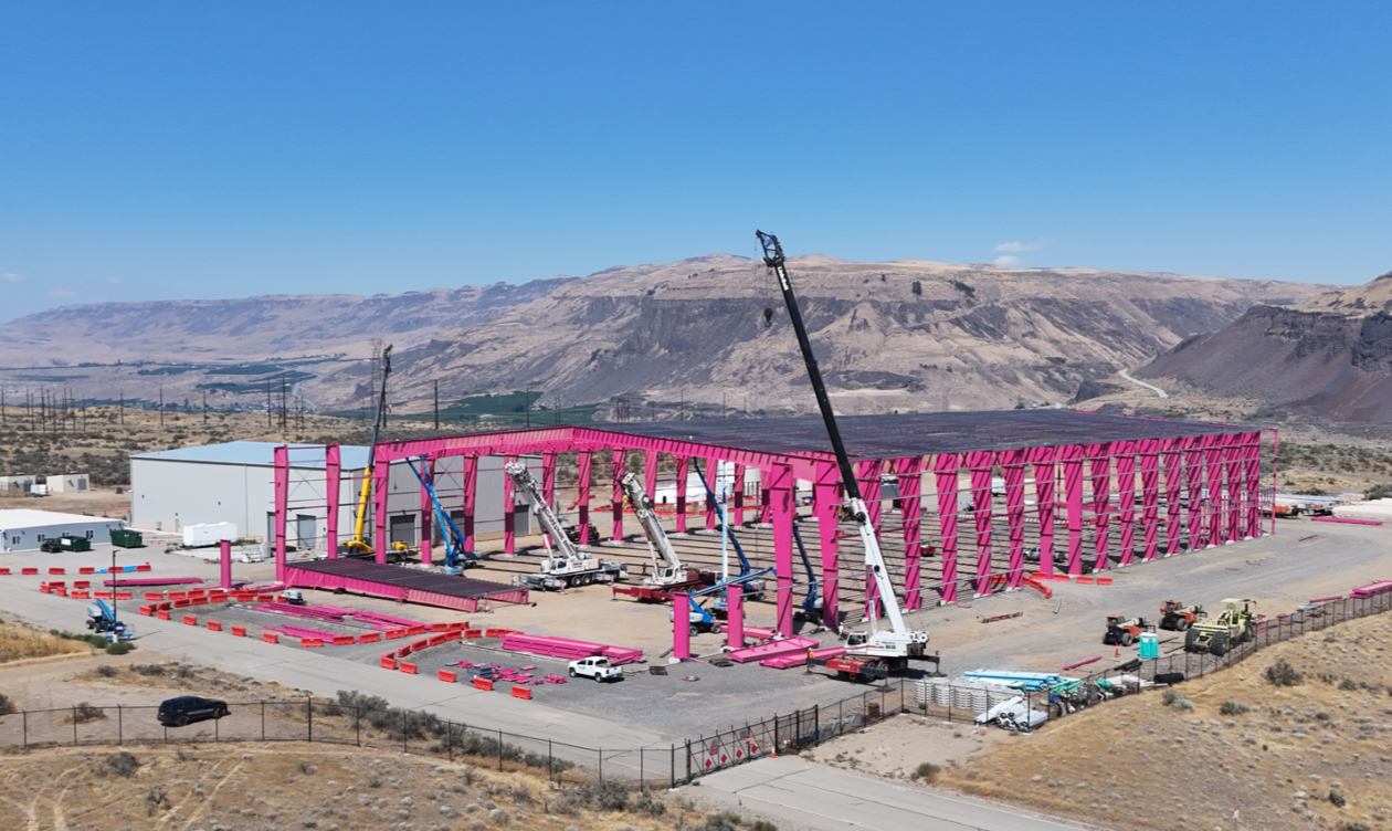
Even as Helion expands into chip manufacturing, the company has not wavered from its original goal. Orion, its commercial-scale fusion plant, is under construction in Malaga, Washington, near the Columbia River. Helion has signed an agreement to supply electricity from that facility to Microsoft, a major vote of confidence in the company’s timeline and technology. Helion is targeting initial operations in 2028, and CEO David Kirtley made it clear in an interview that this schedule remains intact. “So that’s still the plan,” he said. “We’re building Orion components and operating our other systems internally, and the work continues in parallel with all of this.” The construction site in Malaga is a testament to how far Helion has come, but it also highlights how much work remains. Fusion has not yet proven itself as a net source of energy anywhere in the world; dozens of companies are chasing the same breakthrough, and none have so far shown that their machines can produce more power than they consume. Helion is trying to be the first, and the new semiconductor initiative is part of that attempt. Kirtley acknowledged that some of the semiconductors currently available for use in Orion are being sourced primarily from overseas vendors. But he expects that chips developed through the new initiative will be used in Orion as well, potentially late in its construction. That would make Orion something more than a demonstration project: it would be a working example of a new domestic supply chain, built from the ground up by a company that refused to wait for someone else to solve its problems.
The bigger picture is that Helion has chosen to fight on two fronts at once, and it is doing so with a level of ambition that matches the scale of the challenge. Commercializing fusion energy is one of the hardest technical problems humanity has ever attempted. It requires mastering plasma physics, materials science, cryogenics, magnets, and now, increasingly, advanced electronics. The semiconductor program adds another layer of complexity, but also another source of strength. If Helion succeeds, it will not just have built a fusion power plant; it will have helped rebuild a piece of America’s semiconductor manufacturing base, created jobs in Washington state, and demonstrated how a startup can use a federal initiative like the CHIPS Act to accelerate its own private mission. The arrangement between Helion and the Commerce Department is not yet final; the letter of intent is a preliminary step, and the government would receive a non-voting equity interest in exchange for its funding. But the direction is clear. Helion is no longer just a fusion company. It is an energy company, a semiconductor company, and an American manufacturing story, all wrapped into one. As Kirtley put it, “As soon as the award kicks off, we can build out the manufacturing capacity and the testing capacity, and in a parallel, do the research and development into the next generation of semiconductors as well.” That is the language of a person who sees no reason to choose between building a star and building the chips that make it shine.