


Inside the humming, crowded halls of modern data centers, a quiet crisis is unfolding. The machines powering the artificial-intelligence boom are voracious, not just for data but for electricity. They consume so much power and throw off so much heat that operators are running into hard physical limits: there isn’t enough grid capacity, enough cooling, enough room to keep adding more servers. For a long time, the tech industry acted as if the only answer was to build bigger data centers and stronger power plants. But a small startup in Vancouver, Washington, believes the answer is much closer to the chip itself. Powerlattice, founded in 2023, builds a technology that doesn’t try to make AI chips compute faster in the traditional sense; instead, it makes the journey of electricity to those chips radically more efficient. And on Friday, the company revealed a major milestone: it has raised $86 million in new funding, according to an SEC filing. That amount nearly triples the $31 million the company had raised when it emerged from stealth last November, and it signals that investors are beginning to see power delivery, not just processing power, as one of the most important bottlenecks in AI. The problem is one of physics and packaging. Today’s AI accelerators are fed by power regulators that sit at some distance from the processor. The electricity travels along long, winding paths, and in that journey it meets resistance, which turns energy into heat and waste. Powerlattice’s invention is a power delivery chiplet: a small, dedicated piece of silicon that lives inside the processor package, right next to the compute. By shortening the distance from regulator to processor, the chiplet wastes far less energy and lets more power do useful work. The company says this approach can cut energy use by more than half while also boosting performance. For a world that will soon need enormous amounts of electricity just to run AI, that would be like finding a new, clean energy source hiding in the wires.
The new funding round is notable not just for its size but for the credibility of the people and firms behind Powerlattice. The company emerged from stealth last November with a $25 million Series A led by Playground Global and Celesta Capital, two venture firms with deep roots in hardware and semiconductors. On the board sits Pat Gelsinger, the former Intel CEO and now a general partner at Playground. Gelsinger has become one of the most prominent voices warning that power, not computing capacity, will determine how fast AI can grow. His line from last year, “AI is not constrained by capital, it’s constrained by power,” has become a rallying cry for the industry. Steve Fu of Celesta also sits on the board, adding another layer of semiconductor and investment expertise. The SEC filing from late October shows Powerlattice is seeking a total of $111 million, with 18 investors participating so far. The filing does not name those investors, and the company declined to comment, leaving room for speculation about whether strategic partners, chipmakers, or data center operators are among them. But the structure of the raise suggests strong demand and deliberate pacing. For a hardware startup, where product cycles are long and trust is built slowly, nearly tripling its funding in less than a year is a meaningful validation. The money arrives at a moment when the biggest names in tech are publicly scrambling to secure power supplies, announcing nuclear deals, solar agreements, and partnerships with utilities. Powerlattice offers a complementary and perhaps more immediate answer: do more with the electricity we already have. That message appeals to chip designers, cloud providers, and energy-conscious investors alike, and having someone like Gelsinger as a champion gives the company a powerful advocate who understands the gritty realities of semiconductor manufacturing and the strategic importance of the power supply chain.
At the center of Powerlattice’s pitch is a stubborn fact: the electricity that powers a processor has to come from somewhere, and the last few millimeters of its trip are often the most wasteful. In conventional designs, power is delivered from a voltage regulator that is separate from the processor, routed through the motherboard, and then pushed into the chip. By the time the electrons arrive at their destination, a meaningful portion of the energy has already been lost as heat. That heat then requires even more energy to remove, creating a vicious cycle. Powerlattice’s solution is a power delivery chiplet, a compact component designed to be integrated inside the same processor package as the GPU, CPU, or custom accelerator. Rather than traveling a long distance, electricity is converted and regulated right at the point of use. The company says this architectural shift can cut energy consumption by more than half while simultaneously improving performance. Processors that run cooler and receive cleaner power can sustain peak loads for longer periods, which is exactly what AI training and inference demand. A year ago, Powerlattice said it was already providing engineering samples to partners working on GPUs, CPUs, and custom accelerators. That early traction was significant because it meant the team had moved beyond theory and was putting actual silicon into the hands of hardware engineers who could test it against real workloads. The latest milestone, announced just days before the funding news, pushes the concept even further. Powerlattice says it has demonstrated what it calls the industry’s first monolithic integrated voltage regulator chiplet, a single piece of silicon that combines the controller, the power transistors, and the inductors all in one place. Previously, those components were often spread throughout a system, each with its own overhead, cost, and potential for failure. Squeezing them onto one chiplet is a design and manufacturing achievement, and it reduces the size, complexity, and cost of power management while improving reliability.
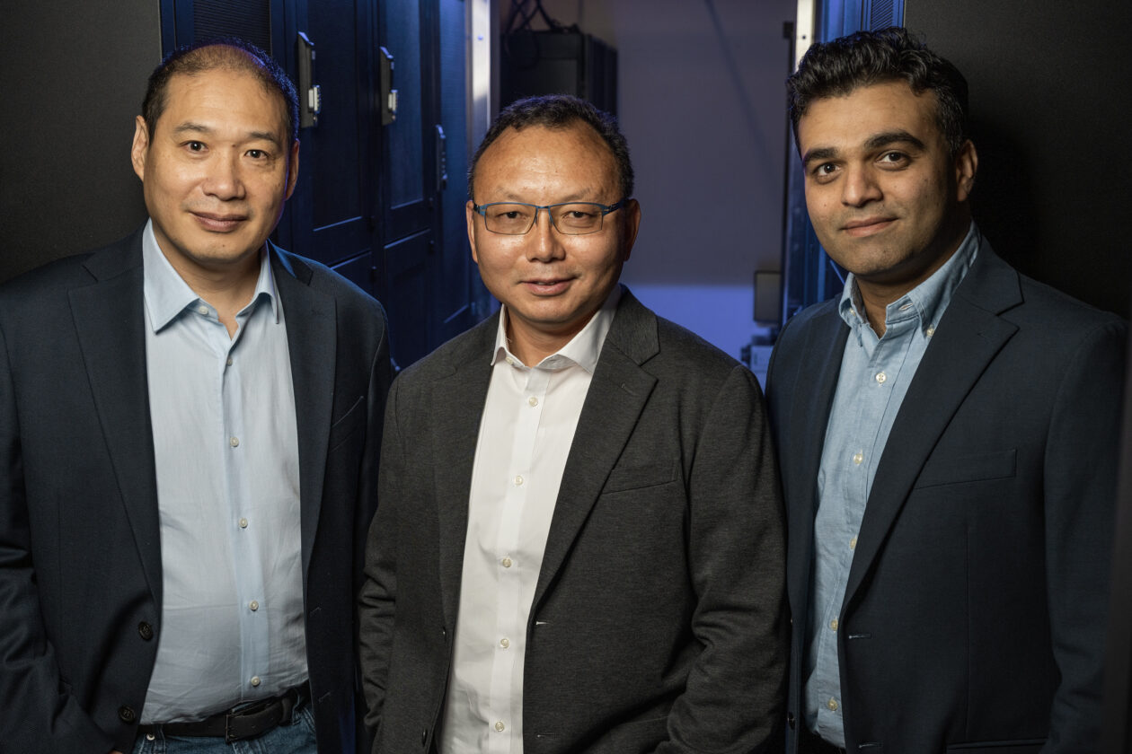
Powerlattice is the kind of company that could only come from people who have spent decades inside the semiconductor industry and emerged with a deep understanding of its pain points. The three founders, CEO Peng Zou, Gang Ren, and Sujith Dermal, started the company in 2023. Their combined resumes read like a tour through the last quarter century of chip design: Qualcomm, Intel, and NUVIA, the well-regarded startup that Qualcomm acquired in 2021 for its processor expertise. That lineage matters. Zou, Ren, and Dermal have not just designed chips; they have lived the compromises between performance, power, and heat that define every generation of silicon. They know that adding more cores or squeezing in more transistors is not enough if you cannot feed the processor with electricity. Seeing them start a company dedicated to power delivery is like watching veteran mechanics decide to build a better fuel line after years of tuning high-performing engines. Their background also gives them credibility in a conservative industry. When a startup says it can cut power use by nearly half, the natural reaction is skepticism. But when the message comes from engineers who have shipped products at Qualcomm and Intel and worked on NUVIA’s advanced designs, the conversation changes. They understand thermal limits, packaging constraints, manufacturing yields, and the brutal economics of producing chips at scale. The company’s footprint reflects the global nature of the chip business. Powerlattice is headquartered in Vancouver, Washington, just across the river from Portland, Oregon, and it also maintains offices in Chandler, Arizona, a major semiconductor hub; San Jose, California, at the heart of Silicon Valley; and Hsinchu, Taiwan, home to the island’s sprawling semiconductor supply chain. That spread allows the company to work closely with customers across the industry, from North American chip designers to Asian manufacturers, and gives it a view of the entire ecosystem.
The recent announcement of the monolithic integrated voltage regulator chiplet is more than a technical footnote; it is a statement of intent. In a test, Powerlattice’s chiplet powered a device the company built specifically to mimic the fast-shifting electrical loads of next-generation AI accelerators. Those loads are the real challenge. AI models draw power in sudden, erratic bursts, spiking when a massive computation hits the GPU, dropping when a layer finishes, and the power system has to respond in microseconds. Any hesitation or inefficiency shows up as heat, wasted energy, or slower processing. The fact that Powerlattice could build a chiplet to handle those swings smoothly, while packaging the controller, transistors, and inductors all on one piece of silicon, is a strong signal that the technology is ready for the demanding reality of actual AI workloads. The modular approach also gives designers flexibility. Instead of forcing every processor into the same power architecture, Powerlattice says multiple chiplets can be linked together and behave as one, effectively allowing a design to be scaled up or down depending on the processor’s appetite. A modest chip might use one chiplet; a massive accelerator could use several, all working in concert. That flexibility is crucial because AI hardware is diversifying rapidly. Nvidia’s GPUs, AMD’s offerings, Google’s TPUs, and a wave of custom accelerators from startups all have different power requirements. Powerlattice’s ambition is to be the layer beneath all of them, a universal answer to the power wall. CEO Peng Zou’s comment in the announcement captures the company’s philosophy: “Breaking through the AI power wall requires us to rethink how power reaches the processor.” It is a reminder that the most important advances are not always the flashiest. Sometimes they are hidden deep inside the machine, in the quiet engineering of power delivery.
What does all of this mean in human terms? It means that the digital services people increasingly rely on, from generative AI assistants to real-time translation, medical research, and autonomous vehicles, will only be sustainable if the infrastructure beneath them becomes radically more efficient. It means fewer data centers needing to be built, less strain on aging power grids, lower energy bills for operators, and a smaller carbon footprint. It also means the AI boom does not have to hit a wall. For years, the industry has operated on a simple assumption: if you want more intelligence, build more chips and give them more power. That equation is breaking down. Powerlattice is part of a wave of companies attacking the other side of the equation, making every watt do more work. The $86 million funding round, which could grow to $111 million as more investors join, gives Powerlattice the resources to turn promising proofs into products. There will still be obstacles. The semiconductor industry is brutally difficult, and many startups have died between a successful demo and a successful product. Powerlattice will need to convince chipmakers to redesign their packages, prove its performance gains at scale, and survive the harsh realities of manufacturing. But the company has attracted serious money, serious mentors, and serious engineering talent. Its story is also a story about the changing nature of computing. The next great leap in AI may not come from a breakthrough in algorithms or a new chip design alone. It may come from paying attention to the humble, invisible path that electricity takes to the processor. In that sense, Powerlattice is not just a chip company. It is a reminder that every intelligent machine has an electrical heartbeat, and that taking care of that heartbeat can make all the difference in the world.